 News
News  Market Data
  Discover
Support: 888-992-3836
Copyright © 2023 InvestorsHub Inc.


Register for free to join our community of investors and share your ideas. You will also get access to streaming quotes, interactive charts, trades, portfolio, live options flow and more tools.
No reading of shorts ‘facts ’was never my strong part. If you are correct it means that one fund had to increase Lightwave by 20% (such a small portion in the weight) so all other sticks in that fund have increased with 20% aswell??
Proof of shit argument shorts this is what this index fund says:
“We use the change in the portfolio allocation because this is the most meaningful metric. Changes can be due to trades or changes in share prices.”
So apparently they do trades…..
You mean the Chips Act isn't dead or dying already like some argued a couple months ago? Idiots believing Fox News propaganda....
Th, TMSC is moving to silicon photonics for co packaged optics solutions. They have understood that semi conductors have reached their physical limits. Smaller is creating more complexity, more heat, ever more expensive to manufacture and is becoming very costly. The combination of electronics and optics by using photons is next leg. Not implying it has anything to do with Lightwave. This is an industry giant understanding they need to change technology to remain relevant. That is great strategic thinking.They use silicon as material, which happens to work well with Lwlg material.
Can you read? Because it literally says "Index Fund".
The only clear and logical answer is that they have partnered with Lightwave logic for polymer modulators integrated into silicon chips. It’s the only way that TSMC would get into photonics.
What else could it possibly be?
#SpiritGuide
Vanguard apparently is as convinced as the longs. Shorts will say it’s index funds… we let them! Great supportive facts that we are on track!
So it seems as though the Linear Pluggable optics is being heralded as the answer ??!!
Nice increases by Vanguard.
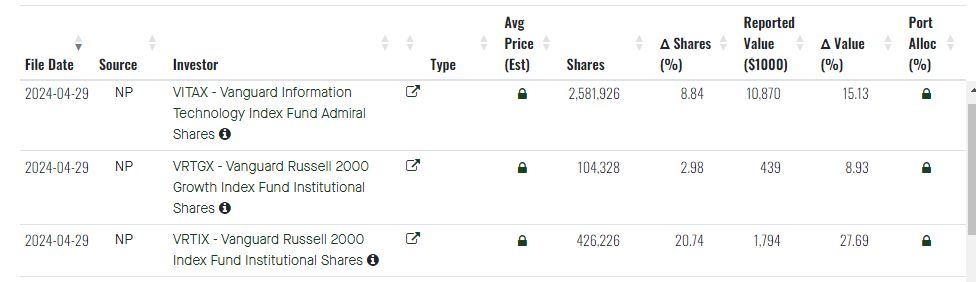
https://fintel.io/so/us/lwlg
th, check it out, a 3rd plant in AZ.. and check those timelines as well.
https://www.tsmc.com/static/abouttsmcaz/index.htm#:~:text=About%20TSMC%20Arizona&text=TSMC%20also%20announced%20plans%20to,greenfield%20project%20in%20U.S.%20history.
Jeunke, yes I read and heard about that. If LWLG polymers was mentioned I would have been buying shares with all my cash.
Mark L is getting paid to promote tfln? Proto is getting paid to promote lwlg? Who knows how many others? The only thing I know is I'm not getting paid to hold this train wreck year after year. Get something commercialized!
WRONG!! the real question is how marky boy comes up with TFLN as his choice to win as the next-gen material when it pretty much sucks in comparison the LWLG materials!! here YOU MUST HAVE MISSED IT because I already asked teddybear to talk to his bff about it
Ha!!! Too funny!!! here teddybear are the FACTS, why don't you get your bff marky boy to answer to the following,
First of all, please tell me if marky boy is being paid to promote TFLN, sure seems like it to me!!!
I only ask this question because TFLN pales by comparison to LWLG Polymers in EVERY competitive aspect, FYI here are the FACTS
1) TFLN is MUCH larger (8 TFLN fit in the space LWLG fits 120 or more)
2) TFLN requires more Voltage and thus CANNOT eliminate the power hungry & expensive Driver chip like LWLG's Polymers
3) TFLN has much high Optical Losses (extremely important in limiting DSP needs)
4) TFLN is not nearly as compatible in Standard Silicon Foundries (if at all!!)
5) and then there was this comment coming back on TFLN from a Silicon Foundry reported by Michael Lebby in the 2023 ASM presentation was this "At our foundry we are worried about the investment into TFLN: it may only be for one generation"
So the FACTS are that LWLG Polymers are clearly the TONS THE BEST solution HANDS DOWN for the Industry today!!!
oh, and btw, many here believe this was the kerrisdale poster that that came on to this message board after the FALSE & MISLEADING report that YOU continued to quote a thousand times even after it was REBUKED SUMMARILY in an SEC FILING!!!!
Th, why do you think TSMC just announced they would get into silicon photonics from 2026 onwards?
After years of globalization US is only No. 1 in chip design. On manufacturing of chips US is not even on No. 2 spot. The chips Act is trying to establish more chips manufacturing capacity in America.
But Intel and TSMC all run into difficulties to open the new facilities, postponing to 2017/2018 now.
Once a country can produce 7 or 5 nm chips most likely would have no problems in design of 3 nm chips. Manufacturing of it requires appropriate machinery.
When the stakes are so high, one way or another, you'll find lots of people with agendas. You and Mark L. are likely to not support the same polymer that most of us here do believe will win in the end. Fine. I wonder though whether the peoples that are "shorting your agenda" are also so noisy on the site where your polymer is being discussed. Is anybody here shorting Paul's Polymer?😂
So lebby had no clue that negotations with a big ass company takes much longer compared to a small tiny company. Lmao Mr. Naive 🤣
Is the optica event available to watch or do you have to be a member?
No one cares who is buying at what price. Where is that knucklehead Khalid who get telling everyone to hold the line. Rumor has it he deserted his post and is now being held in a Siberian prison.
Can’t give you a precise indication. What I see is that the environmental requirements which we see are requiring tremendous changes in the way the big internet companies operate. The competitive situation in the industry is nearing boiling point. Friend and foe are looking for solutions even outside the old boxes,
Radical solutions are necessary. Lightwave’s timing has not changed. When Lebby was asked if the PR 4 december was a mistake? He said:
No, no mistake. In hindsight it would have been better to have communicated that Tier 1’s take more time to decide. It’s a bottom-up and a top down process. It’s a strategic decision and it needs executional effort.
Personally, my interpretation? The announced deals in December are still in the works to be concluded.
When I first invested in LWLG you were speaking out of the other side of your mouth. Beware of opportunists that change their stripes.
Jeunke,
Congats on the new shares. Wish I had more ammo to buy, but out of $$$. Do you think we could hear some good news before the shareholders meeting? Also in your HUMBLE OPINION are we months away from a Contract or partnership, or could it take the rest of the year 2024?
Just bought a nice bunch of shares at fire sale prices.
Apparently not everyone has patience!
Let's get this straight:
( all as per your own words)
You are a very emotional type of "investor", you are only into stocks since a few years, you were long originally, ( decided to buy only after "watching some presentations and reading this forum") then you got impatient and emotional, sold and went short....although you (again as per your own words) "didn't know much about shorting or any other tricks of the trade"
Now you are making claims about Mark L and Dr. Lebby...only trying to influence other people, worthless claims, nothing to do with reality.....
You are a typical short, stupid and/or dishonest and probably both.....
Prov, hope so, but Gallium Nitride is for quantum chips over there.
They are installing "Smart Meters" on homes and I suspect it will give the electric utilities a way to throttle down household usage during high demand. Electric utilities are also offering free "Smart Thermostats" to consumers that definitely give the electric utilities to remotely adjust your electric heating and cooling. I don't live in CA, but I know that last year, they were encouraging people to reduce the use of their AC and discouraging them from charging their electric cars during peak demand. Updating our grid needs to be a top priority, but wind and solar power won't satisfy our growing energy needs. Natural gas isn't going away and we need more nukes.....
Chinese claim gallium arsenide is their photonic solution…
But, it seems obvious going forward, the U.S. will need a solution whose raw materials can be locally sourced (not embargoed in our fruitless war of sanctions) easily integrated into the CMOS process, and malleable enough to be applied to multiple future applications.
TH,
If you look at the spider charts that LWLG has posted, Perkinamine is far and way superior to all these other materials.
Maybe I misinterpreted, but I did not read his comments as “belittling” Lebby. To the contrary, he seemed to me to have been very complimentary of Lebby; but felt, in his opinion, that TFLN would rule the day. Definitely not disparaging.
We are. Somewhere, in a far tiny corner we the solution that is worth 40k so far and solved with by the likes of polariton.
The corner os far away and very small now. But soon it will be bigger and better.
Hope Gallium Nitride made chips would come late, not before LWLG polymers get adopted.
Another one: microwave photonic chips based on lithium niobate crystal.
Not basher or pumper, just try to watch out for my investments here.
Let's get this straight .. mark L ... Respected and well known in the industry.. belittles lebby and puts him in his box with rest of his carrots! And the longs on here start questioning mark L and his credentials???? I can guarantee if mark L had give lebby some positive shout outs then the whole of this board would have been saying how mark L is amazing and well respected in the industry.... Oh .... Looks like the market is running with mark L today though They ain't mugs !!!!
It seems that a good way to talk about the impact our technology would enable would be to make common the metric of “bits per kilowatt hour” as an easily digestible way for the layperson to understand the transformational nature of photonics (specifically EOP).
I’m no mathematician but a 3x improvement in speed, combined with a 90% reduction in power would read like 27x more bits per KW hour.
Good marketing language for Tier 1’s, and the average retail investor.
How about a large investment from a big company to bring this to completion?
Qualcomm invested heavily and publicly in Himax’s 3D optical engine 7 years ago.
https://www.qualcomm.com/news/releases/2017/08/qualcomm-and-himax-technologies-jointly-announce-high-resolution-3d-depth
I just hope we are part of the solution somewhere !! This dead money thing is old
I believe in certain states in the US they will be restricting the electrical usage of citizens long before they throttle down the datacenter electricity consumption.
tkg I believe a 25% data consumption usage is absolutely unattainable as restrictions on data center upgrades would ensue. Our power grid system could not handle that and there would be regulatory pushbacks.
The U.S. power grid is not in good shape. Most of the U.S. power grid system was built in the 1960s and 1970s and currently 70 percent of transmission lines are over 25 years old, getting close to needing replacement. The system is approaching the end of its typical 50–80-year lifecycle. It takes anywhere from 5-15 years to plan, get approval for permits and build out new, more power infrastructure. This process would get speeded up if doing so became more of an urgency but considering the age of our power transmission system, it couldn't happen by 2030.
What this means is that data centers MUST solve a big portion of the power consumption problem and get on the ball sooner than later. Using LWLG technology and Linear-drive Pluggable Optics are both being looked at as options to lower power consumption. For data centers, lowering power is important but functionality will also drive the the choices and we have to wait to see how each technology gets developed.
Thought so; I have a position in OLED and my guy has a target of $210 on it. I've owned LWLG since 2015, my largest position by far. Recent presentations give me a nice security blanket that we own a big winner with LWLG.
yes, because they are in passive organic polymers for displays ( TV, Iphones,computer screen etc) and Lebby often has referenced their business model as being what Lightwave had in mind. Interesting comparison for several reasons. One, the OLED market is dominated by two Tier 1 companies : Samsung and LG, and 2. TV screen saw only a few technical breakthroughs in almost 90 years: Cathode Ray Tubes, Plasma TV, LED , OLED. Organic Polymers.
The Internet saw none yet and in my opinion will opt for organic polymers as well and maybe dominated by a handful of very big companies.
When you refer to OLED, are you saying Universal Display?
Every analyst that covers OLED should cover LWLG. (I'm an old PANL guy)
Very patient, been a shareholder for a while. Just funny no one like Proto isn’t working overtime sending Lebby’s decks to real tech heggies that might take an interest instead of positing the same crap day after day.
Proto, that’s your new project, keep us posted, start with Coatue !!!!!
Just be patient dear, the result will be amazing!
Why don’t you send the slide deck to tech hedge funds, tech investment folks that are looking for massive returns for their shareholders (all accredited investors) like Coatue in NYC, so many others.
www.coatue.com
Seems like they should be on the LWLG bandwagon !
Than we only can hope that the buy-side research analyst visitied lwlg. Hopefully, they will come with a buy reconmendation soon to bring reversal to the down trend lwlg is in.
Hope you guys noticed that the LWLG investor slide deck mentioned 'research analysts' visiting the OFC live demonstrations. In Belgium Michael Lebby told us that these analysts have been following Lightwave seriously since last year's OFC. Analyst attendance kind of neutralizes the argument, often mentionned here, Wall Street would not be seriously interested and would not do any research. To the contrary Wallstreet is interested and is seriously following Lighwave Logic already for quite some time.
|
Followers
|
650
|
Posters
|
|
|
Posts (Today)
|
57
|
Posts (Total)
|
188764
|
|
Created
|
01/06/07
|
Type
|
Free
|
| Moderators pochemunyet prototype_101 Pro_v12001 LOVELWLG JLPTNG Lightning_Rod | |||
The need for Lightwave Logic’s proprietary electro-optic polymers is more evident than at any prior point in history, with internet infrastructure coming under increasing strain due to increased online activity. For example, during the recent COVID-19 pandemic, leading platforms such as YouTube prevented high-definition (HD) streaming in Europe due to data throughput issues in existing internet infrastructure.
The Company’s current focus is on the datacom and telecommunications hardware supply chain for the 100 Gbps and 400 Gbps fiber optics communications market, seeking to integrate its proprietary materials into the devices that comprise key components in today’s internet infrastructure. Lightwave Logic’s unique value proposition, including ease of manufacture relative to traditional solutions, has driven several tier-1 and tier-2 potential strategic partners in the data and telecommunications markets to enter into non-disclosure agreements (NDAs) with Lightwave Logic to evaluate its technology for use in their devices, validating the demand for the Company’s solution in the marketplace. The Company expects to introduce its technology into the commercial marketplace in the near future.
Lightwave Logic is a wholly U.S.-based company with in-house materials synthesis, device/package design, wafer fabrication and testing capabilities at its Englewood, Colorado headquarters.
Having the modulator and integrated circuit development in-house has informed the materials development direction and vice versa. This vertically integrated business model enables a superior platform by aligning the design for manufacturability from materials to complex circuits with the following benefits:
Materials are called electro-optic when they enable interactions between applied electric fields and light passing through them. Notably, they change the refractive index seen by the light with minimum loss. The result is an instantaneous and accurate conversion of an electrical signal to an optical signal. Optical signals are better for transmission over distance: an increasingly useful feature as digital signal speeds are now reaching the GHz and THz ranges and the corresponding electrical transmission distances are shrinking to meters and centimeters.
EO polymers are intrinsically superior in speed and sensitivity to electric field to traditional electro-optic materials such as Lithium Niobate, Indium Phosphide and Silicon. They are engineered materials, made by embedding a variety of specially designed electro-optic chromophore molecules into a wide range of standard host polymers.
Chromophores are complex, large molecules, on a scale akin to drug molecules. They are hyperpolarizable, meaning their electron clouds are easily pulled into a different shape by the applied electric field, changing their optical properties such as index of refraction.
The material is poled to become electro-optic by applying a strong electric field along with heat. The hot material is relatively soft, allowing the chromophore molecules suspended in the host polymer to align in the same direction (poling). Cooling the poled material after the molecules are in place traps them in their active state even after the poling field is removed.

Although the electrons in the material respond to any applied electric field, they remain tightly bound to the molecule. The response to an applied signal is almost instantaneous response and recovery– like that of a tight spring– unlike materials that involve much slower macroscopic movement of free electrons.
Another key difference from traditional crystalline materials is the performance of EO polymers continues to improve as chemists explore the almost unlimited design space. Combinations of chromophores and host polymers can be tailored for specific applications.
In addition to innovating the EO polymer materials, Lightwave Logic takes its technology platform to the next level by developing ancillary materials and processes. These elements are brought together and demonstrated in advanced high-speed optical modulators.
The polymer is spun onto silicon wafers and standard microfabrication techniques are used to deposit and pattern metal electrodes and optical waveguides.
One well-known optical modulator device is the Mach-Zehnder interferometer. The light output is changed by changing the relative phase between the two arms. One common trick to double the effect for the same available drive voltage is to drive the two arms in opposite directions (push-pull mode). Polymers have an interesting advantage over most other electro-optic materials which are crystalline. The direction of polymer’s electro-optic activity is entirely determined by the direction of the applied poling field. By poling the two arms of the Mach-Zehnder in opposite directions, the resulting device automatically has push-pull operation with a single applied signal.

Once the modulator chip is made, it is packaged for mechanical protection and also to ensure signal quality for electrical and optical connections.
Below is a polymer optical modulator with >60 GHz bandwidth packaged with high-speed electrical connectors and optical pigtails.

Inspired by the remarkable record of integrated microelectronics, the opto-electronics industry has great interest in developing photonic integrated circuits (PICS). Photonics refers to devices that manipulate photons—that is, light—rather than electrons.
Even the best individual devices can be made more functional by integrating many together. Integration has many benefits, the most notable being dramatic improvements in size and cost. Yet, photonic integration has only recently come into the spotlight. The primary applications for photonics used to require stand-alone, high performance components such as used for long-haul telecom.
Now, photonic integration has suddenly come into the spotlight as electronic interconnects struggle to keep up with speed increases of electronic chips. Photonics is being looked at to replace electronics in already highly integrated applications such as chip interconnect. Co-packaging of electronics integrated circuits (ICs) with photonic interconnect, considered unlikely a few years ago, is now viewed by many as inevitable. However, this requirement poses new challenges that are acknowledged as difficult and that new technologies will be required to meet them.
P2IC™ (Polymer Photonic Integrated Circuits) are ideally positioned to be one of these new technologies. Lightwave Logic’s devices are made using conventional wafer-scale processing such as used for microelectronics and therefore similarly capable of being integrated. In addition, the polymer microfabrication processes are compatible with other materials platforms such as Silicon Photonics and Indium Phosphide which are now starting to become more integrated. In particular, the Silicon Photonics ecosystem has recently accepted that its roadmap will include adding more and more materials, each for their specific benefits. EO polymers’ speed and voltage advantages are attractive additions to this ecosystem.
A fiber link sends data from a transmitter to a receiver through an optical fiber cable. Lightwave Logic’s technology can be used to make a data modulator, a central function of the transmitter.

Datacenters and high-performance computing (HPC) are two market segments that demand the very highest speed optical fiber communications. The datacenter fiber communications segment includes applications ranging from connections inside hyperscale datacenters to fiber links between datacenter campuses.
Optical fiber communication is the infrastructure that supports internet content through its entire lifecycle, between businesses, consumers and datacenters. Behind the scenes, massive amounts of data move between computer processors inside datacenters (or inside supercomputers) as content is generated. In addition to these intra-datacenter links, there are also significant datacenter interconnection links between big datacenters to provide flexible capacity and resilience – all of these represent significant addressable market segments for Lightwave Logic’s technology.


Modulator performance limits the speed of the transmitter, which in turn limits the data-carrying capacity of the entire fiber link. EO polymers have superior speed and sharply reduce the electrical power needed to operate the modulators.
Lightwave Logic estimates that in 2019, the total market for opto-electronic components used in the fiber optics market reached a value of ~$26 billion and is forecasted to grow to approximately $80 billion by 2030.

Above: Market forecasts for photonic (electro-optic) components and transceivers used in optical fiber communications. (Source: Oculi LLC)
The growth in the optical fiber communications market is driven by many factors, primarily:
The historic trend has been a migration from text to graphics, followed by still graphics to increasingly high-definition video. On the accessibility front, the introduction of 5G will enable low-cost mobile internet connections at the same, or higher speeds, as today’s home broadband. This trend continues today as users demand more data at all times.
Recently, particularly since the onset of the COVID-19 pandemic, there has been a sharp increase in reliance on video-conferencing services, often replacing in-person meetings. As video conferencing becomes more commonly used, users will continue to demand faster response times to enable no-lag, real-time communications in full HD.
The benefits of EO polymers, such as low power usage, high speed, increased throughput and lower cost make them ideally suited for markets outside of communications as well, including in consumer, media, augmented reality/virtual reality, medical and industrial applications.
Developing, protecting and commercializing intellectual property is central to Lightwave Logic’s identity as a technology company. Lightwave Logic has over 50 U.S. and international patents and applications that are issued or pending.
These patents provide freedom of manufacture for the company’s electro-optic (EO) polymer materials systems and its optical device technology.
Lightwave Logic’s patent portfolio covers the following areas:
The company continuously seeks to innovate new electro-optic chromophores, designing molecular architectures to meet application needs such as high electro-optic activity and stability. We also design ancillary materials that are useful in conjunction with the EO polymers themselves. Example patents within the materials category include:
| Publication Number | Title |
|---|---|
| US Patent 7,902,322 | Nonlinear optical chromophores with stabilizing substituent and electro-optic devices |
| US Patent 9,535,215 | Fluorinated Sol-Gel Low Refractive Index Hybrid Optical Cladding and Electro-Optic Devices Made Therefrom |
As the company demonstrates its materials in devices, such as modulators, it has engineered ways to enhance device performance by means of device design and optimized control. Example patents within the optical device category include:
| Publication Number | Title |
|---|---|
| US Patent 10,520,673 | Protection layers for polymer modulators/waveguides |
| US Patent 7,738,745 | Method of Biasing and Operating Electr-Optic Polymer Optical Modulators |
Materials innovations are followed by methods in which the Company or its partners can best work with the materials in the fabrication process. Example patents within the fabrication category include:
| Publication Number | Title |
|---|---|
| US Patent Application 20190353843 | Fabrication process of polymer based photonic apparatus and the apparatus |
| US Patent 10,591,755 | Direct-drive polymer modulator methods of fabricating and materials therefor |
Polymers can be used to add functionality to existing semiconductor devices, inclusive of making photonic integrated circuits (ICs). Areas of active innovation include how to get light from one material system into another with minimal losses. Example patents within the semiconductor integration category include:
| Publication Number | Title |
|---|---|
| US Patent 10,527,786 | Polymer modulator and laser integrated on a common platform and method |
| US Patent 10,511,146 | Guide transition device with digital grating deflectors and method |
Challenges for high-speed optical packaging includes maintaining the quality of radio-frequency electrical signals and hermetic/environmental sealing of devices for durability (while still allowing light to go through). Example patents within the packaging category include:
| Publication Number | Title |
|---|---|
| US Patent 10,574,025 | Hermetic capsule and method for a monolithic photonic integrated circuit |
| US Patent 10,162,111 | Multi-fiber/port hermetic capsule sealed by metallization and method |
We cannot assure you that we will meet the conditions of the 2023 Purchase Agreement with Lincoln Park in order to obligate Lincoln Park to purchase our shares of common stock, and we cannot assure you that we will be able to sell any shares under or fully utilize the Roth Sales Agreement. In the event we fail to do so, and other adequate funds are not available to satisfy long-term capital requirements, or if planned revenues are not generated, we may be required to substantially limit our operations. This limitation of operations may include reductions in capital expenditures and reductions in staff and discretionary costs.

| Volume | |
| Day Range: | |
| Bid Price | |
| Ask Price | |
| Last Trade Time: |


